

In Caring circuit, there are two options for pcb stackup design suggestions:
1. Leave it to caring circuit to design PCB stackup for you (Recommended)
Why?
- You don’t need to spend your time by designing stackup. Leave it on Caring Circuit – We are professionals. We do it everyday. Also, you can work on design in parallel of handling issues with PCB stackup.
- Many times Caring circuit is not able to build PCB stackup designed by other company or a person outside their company. The main reason is unavailability of material used in some PCB stackups. Selection of material is the best to leave on them – We will choose stocked material and know how to save cost for customer.
- Caring circuit knows how to design could be manufacturable and keep rejected boards rate as low as we can.
- Caring circuit use different track geometry calculators and Caring Circuit will not guarantee track impedance value if track geometry is calculated by someone else. Many times caringcircuit calculated numbers and customer’s calculated numbers will be different because of different materials or brands.
An example of email to Caring circuit with request for PCB stackup and track geometry:
Please suggest PCB stackup and track geometry for PCB with following parameters:
PCB Description
12 Layers:
L1 – Signal
L2 – GND
L3 – Signal
L4 – Signal
L5 – GND
L6 – Powers
L7 – Powers
L8 – GND
L9 – Signal
L10 – Signal
L11 – GND
L12 – Signal
Please suggest stackup.
Required impedances:
Single ended: 50 OHMs (L1 (Ref: L2); L3, L4 (Ref: L2, L5); L9, L10 (Ref: L8, L11); L12 (Ref: L11))
Differential: 70, 90, 100 OHMs (L1 (Ref: L2); L3, L4 (Ref: L2, L5); L9, L10 (Ref: L8, L11); L12 (Ref: L11))
Please suggest geometry for impedance controlled tracks: Track width / Gap
Used VIAs:
Through hole VIA: 0.35mm (pad) / 0.22mm (drill),
Start layer: L1, End layer: L12
VIAs:
Start layer: L1, End layer: L2; 0.27mm (pad) / 0.1mm (laser drilled hole)
Start layer: L2, End layer: L3; 0.27mm (pad) / 0.1mm (laser drilled hole)
Start layer: L10, End layer: L11; 0.27mm (pad) / 0.1mm (laser drilled hole)
Start layer: L11, End layer: L12; 0.27mm (pad) / 0.1mm (laser drilled hole)
Buried VIA:
Start Layer: L3, End layer: L10; 0.45mm (pad) / 0.2mm (drill)
Other:
Minimum track: 0.12mm / Minimum gap: 0.12mm
Board thickness: 1.6mm +/- 10%
Board size: 100x200mm
2. Design PCB stackup by yourself
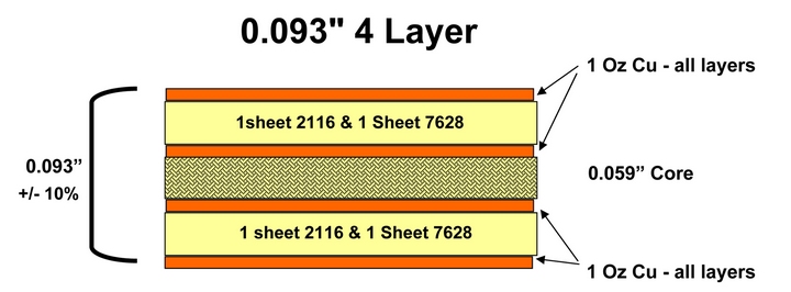
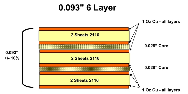
1) Multilayer circuit boards comprise outer and inner layers (copper layers) and help to achieve more complex, denser wiring structures.Basic information about PCB stackups for your information:
- PCB is grouted using three components: Copper foil, Prepreg, Core
Copper foil
Prepreg ( pre-impregnated fibre glass/ resin composites)
Core (prepreg grouted between 2 copper foils)
Prepregs and cores are also available in High-Tg and halogen-free types.
- Standard Copper foil thickness: 5um, 12um, 18um, 35um, 70um
- Standard prepreg thickness: 65um, 100um, 180um
- Standard core thickness: 0.15mm, 0.20mm, 0.36mm, 0.46mm, 0.56mm, 0.71mm, 1mm, 1.2mm, 1.5mm, 2.0mm, 2.4mm, 3.2mm. Core is supplied with copper foil on both sides. For some cores you need to add copper foil thickness (18um or 35um) to the core thickness.
2) The following are sample layer buildups for circuit boards prototypes. Since we always manufacture depending on customer specifications and in-stock materials, which may lead to an alternate buildup, please always consult with our technicians about critical layer buildups. There are some rules how to build your stackup. Not every combination is possible. Check it out with Caring circuit. Note: If you calculate impedances for your own stackup, don’t forget about PLATING. Plating process add an additional copper (e.g. 20um) to top and bottom layer (or if you use uVIAs and buried VIAs, then also to some of the inner layers).


3) Following are material we have in stock for your reference when you design your stackups.
Prepregs
We have the following FR4 prepregs in stock:
The following FR4 prepregs are partially in stock, or are available for order:
|
CCL:
| Thickness | Copper thickness |
|---|---|
| 50µm | 18µm/18µm; |
| 100µm | 18µm/18µm; 35µm/35µm |
| 150µm | 18µm/18µm; 35µm/35µm; 70µm/70µm; 105µm/105µm; |
| 200µm | 18µm/18µm; 35µm/35µm; 70µm/70µm; 105µm/105µm; |
| 300µm | 18µm/18µm; 35µm/35µm; 70µm/70µm; 105µm/105µm; 140µm/140µm; |
| 350µm | 18µm/18µm; 35µm/35µm; 70µm/70µm; 105µm/105µm; 140µm/140µm; 210µm/210µm |
| 400µm | 18µm/18µm; 35µm/35µm; 70µm/70µm; 105µm/105µm; 140µm/140µm; 210µm/210µm |
| 500µm | 18µm/18µm; 35µm/35µm; 70µm/70µm; 105µm/105µm; 140µm/140µm; 210µm/210µm |
| 550µm | 18µm/18µm; 35µm/35µm; 70µm/70µm; 105µm/105µm; 140µm/140µm; 210µm/210µm |
| 600µm | 18µm/18µm; 35µm/35µm; 70µm/70µm; 105µm/105µm; 140µm/140µm; |
| 700µm | 18µm/18µm; 35µm/35µm; 70µm/70µm; 105µm/105µm; 140µm/140µm; |
| 800µm | 18µm/18µm; 35µm/35µm; 70µm/70µm; 105µm/105µm; 140µm/140µm; |
| 900mm | 18µm/18µm; 35µm/35µm; 70µm/70µm; 105µm/105µm; |
| 1000µm | 18µm/18µm; 35µm/35µm; 70µm/70µm; 105µm/105µm; |
| 1200µm | 18µm/18µm; 35µm/35µm; 70µm/70µm; 105µm/105µm; |
| 1500µm | 18µm/18µm; 35µm/35µm; 70µm/70µm; 105µm/105µm; |
| 2000µm | 18µm/18µm; 35µm/35µm; 70µm/70µm; 105µm/105µm; |
| 2400µm | 18µm/18µm; 35µm/35µm; 70µm/70µm; 105µm/105µm; |
| 3200µm | 18µm/18µm; 35µm/35µm; 70µm/70µm; 105µm/105µm; |
*Special cores may also be pressed for a particular project.
Copper foil
| 12µm | 18µm | 35µm | 70µm | 105µm | 210µm |